A new technique developed by researchers could solve one of the biggest challenges in making future computer chips from ultrathin materials. The breakthrough involves coating molybdenum disulfide — a promising semiconductor material just three atoms thick — with oxygen or fluorine, allowing manufacturers to remove precisely just the top layer of atoms during plasma processing. The result is a cleaner, more controlled path toward smaller and more capable computer chips.
The Challenge
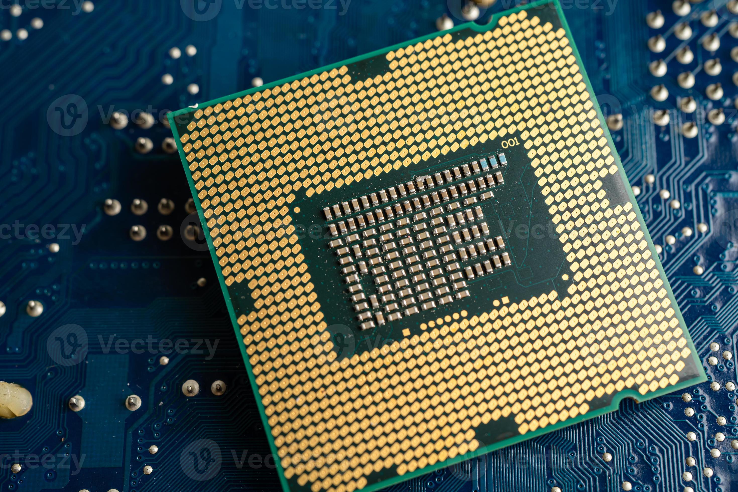
As traditional silicon-based transistors approach their physical limits, the semiconductor industry has been exploring new materials that can continue the trend of miniaturisation. Molybdenum disulfide (MoS₂) is one of the most promising candidates — it is atomically thin, flexible, and has excellent electronic properties. However, manufacturing chips from such thin materials is extraordinarily difficult.
Plasma processing, a standard technique in semiconductor manufacturing, can easily destroy or damage atomically thin materials. The new technique addresses this by creating a protective layer that shields the underlying material while allowing precise removal of the top atomic layers.
How It Works
| Method | Traditional | New (Coated) |
|---|---|---|
| Material | Bulk silicon | Monolayer MoS₂ |
| Processing | Plasma etching | Oxygen/fluorine coating + plasma |
| Precision | ~10nm granularity | Single-atom precision |
| Damage risk | Low (thick material) | Low (coating protects) |
| Scalability | Proven | Promising early results |
Implications for India's Semiconductor Ambitions
India's push to become a semiconductor manufacturing hub — through the India Semiconductor Mission and partnerships with global chip makers — could benefit from this breakthrough. If the technique proves commercially viable, it could accelerate the adoption of next-generation chip materials in Indian fabrication facilities.
India's growing semiconductor ecosystem, including the planned fabrication units in Gujarat and Assam, will need access to the latest manufacturing techniques to remain competitive. Research institutions like IIT Bombay and IIT Madras are actively collaborating on similar nanoscale materials research.
Limitations
The research is still at the laboratory proof-of-concept stage. Commercial adoption would require scaling the coating process to wafer-level production, validating the technique across different chip designs, and integrating it into existing fabrication workflows. Industry experts estimate it may take 5-7 years before the technique appears in commercial chip manufacturing.
Sources
- ScienceDaily: Top Science News — Plasma chip technique
- ScienceDaily: Latest Research News
- University of Minnesota: New plasma processing technique for 2D materials